photomask.
Photomask business|Photomask introduction
introduce.
Photomask introduction
The photomasks produced by Finex are for the high precision industry.
Photomasks are produced by forming delicate 2–3µm patterns on the glass board. Customers use our photomasks to produce flat panel displays similar to liquid crystal. Flat panel displays such as liquid crystal and plasma are widely used for TVs, PCs and mobile phones.
SK-Electronics, the parent company of Finex, has been actively developing technologies to meet large-size, high-precision demand since 1980s. In recent years, SK-Electronics has been able to provide 1 m2 large photomask for the 10th generation LCD panel.
manufacturing process.

applied field.
Field of application
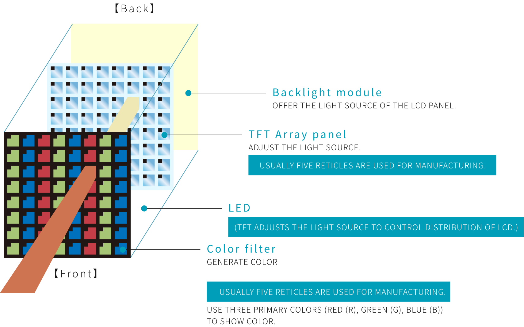
The photomasks produced by Finex are primarily for TFT (Thin-Film Transistor) and CF (Color Filter).
・TFT (Thin-Film Transistor)・
It is one of the liquid crystals formed by thin-film transistors. It is a transistor on a glass substrate formed by a-Si, LTPS and IGZO. It can be used for LCD panels.
・CF (Color Filter)・
In order to display color on the LCD, pigment is added to the resin film, which is one of the ingredients of the liquid crystal component. Patterns in red, green and blue will then formed orderly on a transparent glass substrate.

introduce of gtm./htm.
Multi-gray scale photomask
■ Residual film control and PEP saving application technology
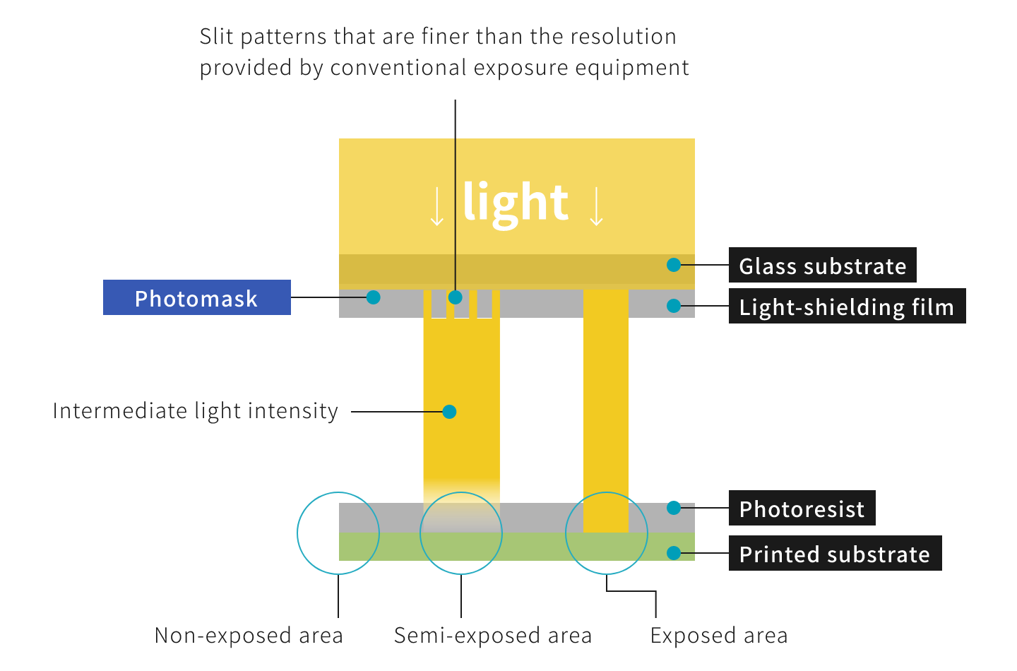
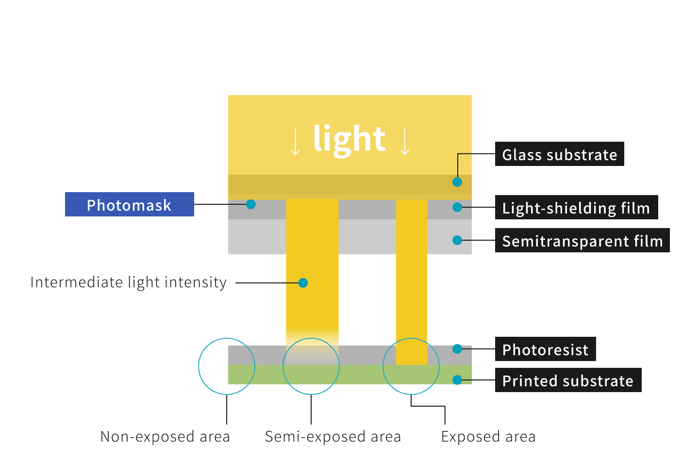
Multi-gray scale photomask can be divided into gray-tone mask and half tone mask. Gray-tone mask generates the slit with lower resolution in contrast to the aligner and covers part of the light to achieve semi-exposure. On the other hand, half-tone mask uses semi-transparent film to achieve semi-exposure.
Since both methods above can generate three conditions, “exposure”, “semi-exposure” and “non-exposure” after one exposure. Therefore, the photoresist can have two different thickness (sensitizer) after development. The difference of photoresist thickness can transcribe the pattern to the panel substrate with less Photomask in general, and improve production efficiency of panel.
Gray-tone mask

Half-tone mask

introduce of dc.
DC photomask application
■ The ideal lattice photomask is placed on the aligner for exposure production.
When the ideal lattice photomask is placed on the aligner for exposure, the glass substrate may appear unexpected lattice shape due to the performance of the optics and the aligner itself, which will affect the registration accuracy in different layers. DC photomask conducts reverse compensation based on the exposure feature and shape of each aligner and the shape difference of the array and CF substrate. The exposure result meets the criteria of ideal lattice and enhances registration accuracy.

introduce of psm.
PSM photomask
■ Another breakthrough in exposure resolution capabilities
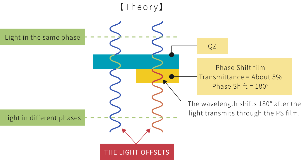
PSM is the Phase Shift Mask. The original Cr film will be replaced by phase shift film, hereinafter referred to as PS film.
The feature of this material is that when light penetrates the glass and PS film, the wavelength of the light will have a phase-shist of 180°. This phase difference can enhance photoresist intensity in the exposure area of the panel and the design of thin CD will make the pattern easier to resolved.
Therefore, the photomask with this phase difference can enhance and improve resolution of the aligner.
The PSM product can be divided into Only PSM and Rim PSM (Cr+PS).
It can suggest the adequate type and optimize resolution based on the design of the customer’s pattern or CD.
